Synthesis of Photoactive Ternary Cadmium Sulfoselenide Thin Film via Cost-effective Chemical Technique for Solar Cell Application-Juniper Publishers
JUNIPER
PUBLISHERS- ACADEMIC JOURNAL OF POLYMER SCIENCE
Abstract
We have successfully developed arrested precipitation technique for synthesis of photoactive Cd(S0.8Se0.2)
thin film. Synthesized thin film were characterized for optical,
structural, morphological and compositional analysis using UV–Vis
spectrophotometer, Xray Diffraction (XRD), Field-Emission Scanning
Electron Microscopy (FESEM) and Energy Dispersive Spectroscopy (EDS)
analyzer techniques. Optical study shows linear nature of plot confirms
direct allowed transition with optical band gap energy 2.13eV. Pure
phase hexagonal nanocrystalline thin film formation confirmed through
XRD pattern. FESEM micrographs indicate construction of void free and
well-adherent twisted nest-like surface morphology containing tremendous
grown flakes over substrate. Presence of Cd2+, S2- and Se2- elements
confirmed by EDS spectrum. Finally, synthesized thin film show power
conversion efficiency of 0.37 %.
Keywords: APT; Nanocrystalline; n-CdSSe; Thin film; Pure phase; η = 0.37%
Abbrevations:
XRD: Xray Diffraction; FESEM: Field-Emission Scanning Electron
Microscopy; CBD: Chemical Bath Deposition; CCGP: Controlled Chemical
Growth Process; APT: Arrested Precipitation Technique
Introduction
In past few years, the world serious energy and
environmental crisis have made more attention to development of new
cost-effective and sustainable energy source [1]. Also, quest for new
alternative renewable energy source is quite argent and necessary.
Overall available technologies photoelectrochemical solar cell
technology has believed to be cost-effective and renewable energy source
for solar energy conversion. Generally, photoelectrochemical
performance of semiconducting materials depends on their respective
properties and essential physiochemical processes in which, i)
Absorption of light radiations, ii) separation of charge carriers, iii)
migration of carriers, iv) recombination of charge carriers and v) redox
reaction. Also, respective properties of semiconducting material are
nothing but, electronic band structure, crystal structure, chemical
constituents and their microstructures.
II-VI group semiconducting compounds are the most
important and highly studied semiconducting material for
scientific and technological point of application due to their direct
band gap [2]. Among this II-VI group semiconducting compounds, typically
CdS and CdSe have 2.40 and 1.70 eV optical band gap with wide
absorption band edge and excellent absorptivity in visible region [2].
These ternary CdSSe thin films synthesized by varied
of method such as, sputtering [3], Chemical Bath Deposition (CBD) method
[4]and solvathermal route [5]. All these methods require highly
sophisticated instruments, harsh experimental condition, different
surface directing agents and solvents [6]. However, in Arrested
Precipitation Technique (APT) their no need to use sophisticated
instrument, different solvents and harsh experimental condition. Taking
into concern these features of technique, we have used APT method for
synthesis of CdSSe thin films. APT method is nothing but hybrid chemical
process of CBD and Controlled Chemical Growth Process (CCGP) [7].
In present investigation, we have successfully deposited
Cd(S0.8Se0.2) thin film using triethanolamine as complexing agent at
via APT method. Our intension is to make efficient photoelectrode
for photoelectrochemical application using triethanolamine as
surface directing agent. Synthesized thin film show 0.37% power
conversion efficiency under illumination of 500W tungsten
filament lamp (intensity 30mW cm-2). Also, thin film formation
growth process by using APT is discussed detailed.
Experimental
Chemicals
All chemicals were of analytical reagent (AR) grade and
used without further purification. Cadmium sulfate hydrate
(CdSO4.H2O) (98%, S-D Fine Chem.), thiourea (H2N-CS-NH2)
(99%, S-D Fine Chem.) selenium metal powder (99.5%, Sigma
Aldrich), sodium sulfite (Na2SO3) (96%, S-D Fine Chem.), liquor
ammonia (NH3) (28-30% Thomas Baker), and triethanolamine
(N(CH2CH2OH)3) (99%, Merck).
Synthesis of Cd(S0.8Se0.2) thin film
In typical synthesis, initially Cd-TEA complex was prepared by
triturating ‘Cd’ with TEA as complexing agent for 6 h homogenous
crushing to form clear Cd-TEA complex. All metal ions and
chalcogen ions precursors’ concentration is optimized at initial
stage of synthesis as 0.05M. Cd-TEA complex release Cd2+ metal
ions slowly and react with S2- and Se2- chalcogen ions released from
dissociation of H2N-CS-NH2and Na2SeSO3 at alkaline pH, 10.4, and
50±2 °C bath temperature at 2.30h deposition time. Formation of
thin films is well dependant on various preparative parameters
such as, deposition time, bath temperature, pH and precursor
concentration. These parameters were optimized during initial
stage of thin film synthesis.
After desired deposition time deposited film was removed
from bath and washed with double distilled water and dried at
room temperature in air. Deposited film was yellowish red in
colour and designated as Cd(S0.8Se0.2).
Characterization of thin film
Thickness of film was measured using surface profiler
(AMBIOS XP-1). Optical absorption spectra were taken by using
a UV-Vis-NIR spectrophotometer (Shimadzu, UV-1800). Structural
properties and crystallite size were carried out using an X-ray
diffractometer (Bruker AXS, D8) using Cu Ka (l= 1.5418 Å). Surface
morphology and the elemental composition of the as-deposited
thin films were characterized using field-emission scanning
electron microscopy (FESEM) equipped with an energy dispersive
X-ray spectroscopy (EDS) analyzer (Hitachi, S-4700). PEC
measurements were carried out using a semiconductor parameter
analyzer (Keithley SCS-4200 Semiconductor) characterization
unit using 500 W tungsten filament lamp (intensity 30mW cm-2)
with sulfide/polysulfide electrolyte.
Results and Discussion
Formation Growth mechanism
Main principle behind the film formation is slow ion-byion
condensation of ions followed by multi nucleation process.
Precipitation of metal chalcogenide thin films is occurred when
ionic products (Kp) of Cd2+, S2- and Se2- ions exceed solubility
product (Ksp) of Cd(SSe) in films. Slow release of metal and
chalcogen ions from respective complex results into highquality
and well-adherent thin films formation [7-9].
Optical absorption studies
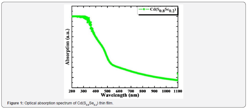
Figure 1 shows optical absorption spectrum of Cd(S0.8Se0.2)
thin film recorded using UV-VisNIR spectrophotometer in 200-
1100nm wavelength range. Maximum light absorption edge
observed at 650nm. Fundamental absorption corresponds to
electron excitation from valance band to conduction band, used
to determine value of optical band gap energy. Optical data were
demonstrated using following eq. (1) as follows,

where, A is a parameter that depends on the transition
probability, h is Planck constant, Eg is optical band gap energy
of material, and exponent depends on the type of transition.
The values of n for direct allowed, indirect allowed, direct
forbidden and indirect forbidden transitions are 1/2, 2, 3/2 and
3, respectively (Figure 1).
From optical absorption spectrum clearly demonstrated
that linear nature of plot confirms direct allowed type transition
mechanism.
Figure 2 shows plot of (ahϑ)2 vs photon energy (hϑ), value
of optical band gap was calculated by extrapolating straight-line
portion to X-axis. Obtained optical band gap energy is 2.13 eV,
which is consistent with other reported ternary CdSSe thin films
[7]. 3.3. X-ray diffraction study
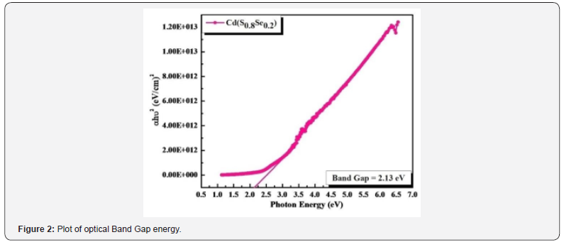
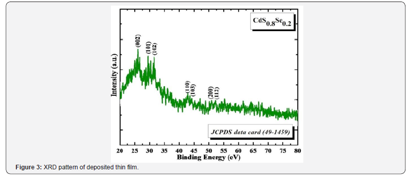
Figure 3 indicates typical X-ray diffraction pattern of
Cd(S0.8Se0.2) thin film deposited by using APT method. All
diffraction peaks are corresponding to (002), (101), (102),
(110), (103), (200) and (112) at 2θ 26.02º, 28.40º, 31.13º,
42.80º, 44.93º, 50.89º and 52.07º of hexagonal crystal structure.
Calculated d-values are in well-agreement with standard d-values
(JCPDS card no. 49-1459) for an (hkl) plane, confirms formation
of thin films with a pure phase material.
Crystallite size is calculated by using known Scherrer formula
and calculated crystallite size is 55nm. Thickness of thin film is
728nm measured by using surface profiler analysis. Crystalline
nature and phase pure formed thin films are highly favorable for
enhanced light absorption in solar cell application [8].
Field emission scanning electron microscopy
Surface morphology of thin films carried out by using FESEM
study. Figure 4 demonstrates FESEM micrographs at different
resolution of Cd(S0.8Se0.2) thin film. Low resolution FESEM
image of Figure 4 (a) point out void free and well adherent film
formation occurs via APT method. It shows twisted nest-like
surface morphology is observed overall substrate surface.
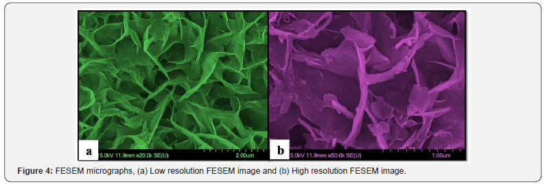
High resolution FESEM images of Figure 4(b) clearly illustrate
that twisting of nest-like morphology with irregularly grown
sharp edged flakes. Such huge number of flakes winds together
and formation of large network of nest-like morphology is
observed from high resolution micrograph. This obtained surface
morphology is beneficial for improve light absorption potential
may due to crystalline nature and large surface area of nest-like
morphology with twisted flakes [9].
Energy dispersive spectroscopy
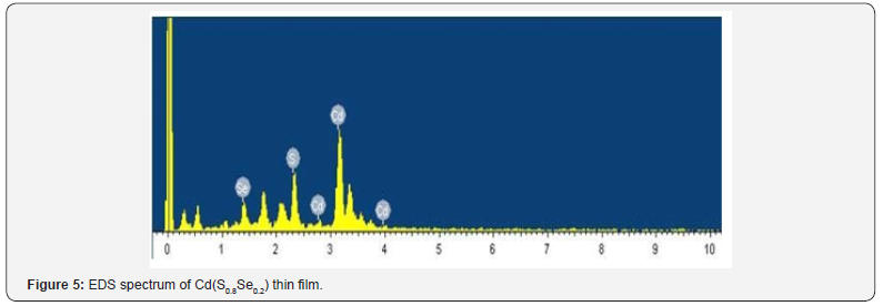
Quantitative analysis of element is confirmed through EDS
study. Figure 5 shows typical EDS spectrum of deposited thin film.
EDS spectrum shows peaks at 3.13, 2.50 and 1.38 keV confirm the
presence of Cd, S and Se elements respectively [7].
Photoelectrochemical performance
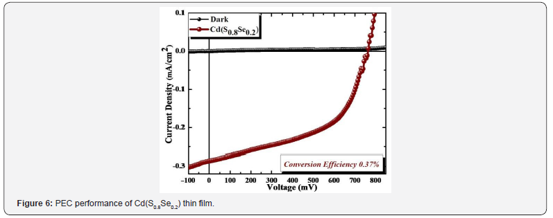
PEC performance of Cd(S0.8Se0.2) thin film was measured with
standard two-electrode system. Figure 6 shows J-V curve of PEC
cells. PEC performance was measured by forming Cd(S0.8Se0.2) thin
film as working photoelectrode with active area 1cm2 and graphite
rod (G) as counter electrode in 0.5M sulfide/polysulfide redox
electrolyte. J-V measurements were done under illumination of
light using 500 W tungsten filament lamp (Intensity of 30mW/
cm2). In dark, J-V curve shows diode-like rectifying characteristics.
Upon illumination, curve is obtained at fourth quadrant, indicating
generation of electricity and n-type conductivity nature [6-7].
Fill factor (FF) and power conversion efficiency (η %) of thin
film were calculated by using equations (2) and (3) as follows,


where, Jmax and Vmax are maximum short-circuit current density
and maximum open circuit voltage, Pin is input light intensity
(30mW/cm2). Jsc is short-circuit current density and Voc is open
circuit voltage. From J-V measurement, short circuit current density
(Jsc) is 0.288mA cm-2 and that of open circuit voltage (Voc) 765mV.
Calculated power conversion efficiency is 0.37% for Cd(S0.8Se0.2)
thin film. Overall obtained conversion efficiency might be due to
good crystallinity and developed surface morphology with large
surface area [9]. Table 1 shows calculated PEC parameter.
Conclusion
Developed facile, cost-effective APT method shows potential
for synthesis of thin films for solar cell. Synthesized thin film
show promising properties favorable for photoelectrochemical
performance is investigated. Optical study showed light absorption
in visible region of solar spectrum and direct allowed transition
mechanism. From XRD pattern it confirmed that formation of
pure phase hexagonal crystal structure with nanocrystalline
nature. FESEM analysis demonstrated synthesized surface
morphology is void free and having large surface area for efficient
light absorption. EDS pattern confirmed presence of Cd2+, S2- and
Se2- elements in synthesized thin film. PEC performance indicated
conversion efficiency of 0.37%.
For more articles in Academic Journal of Polymer
Science please click on:
https://juniperpublishers.com/ajop/index.php
https://juniperpublishers.com/ajop/index.php


Comments
Post a Comment